Back to blog
Article/ Industry Insights
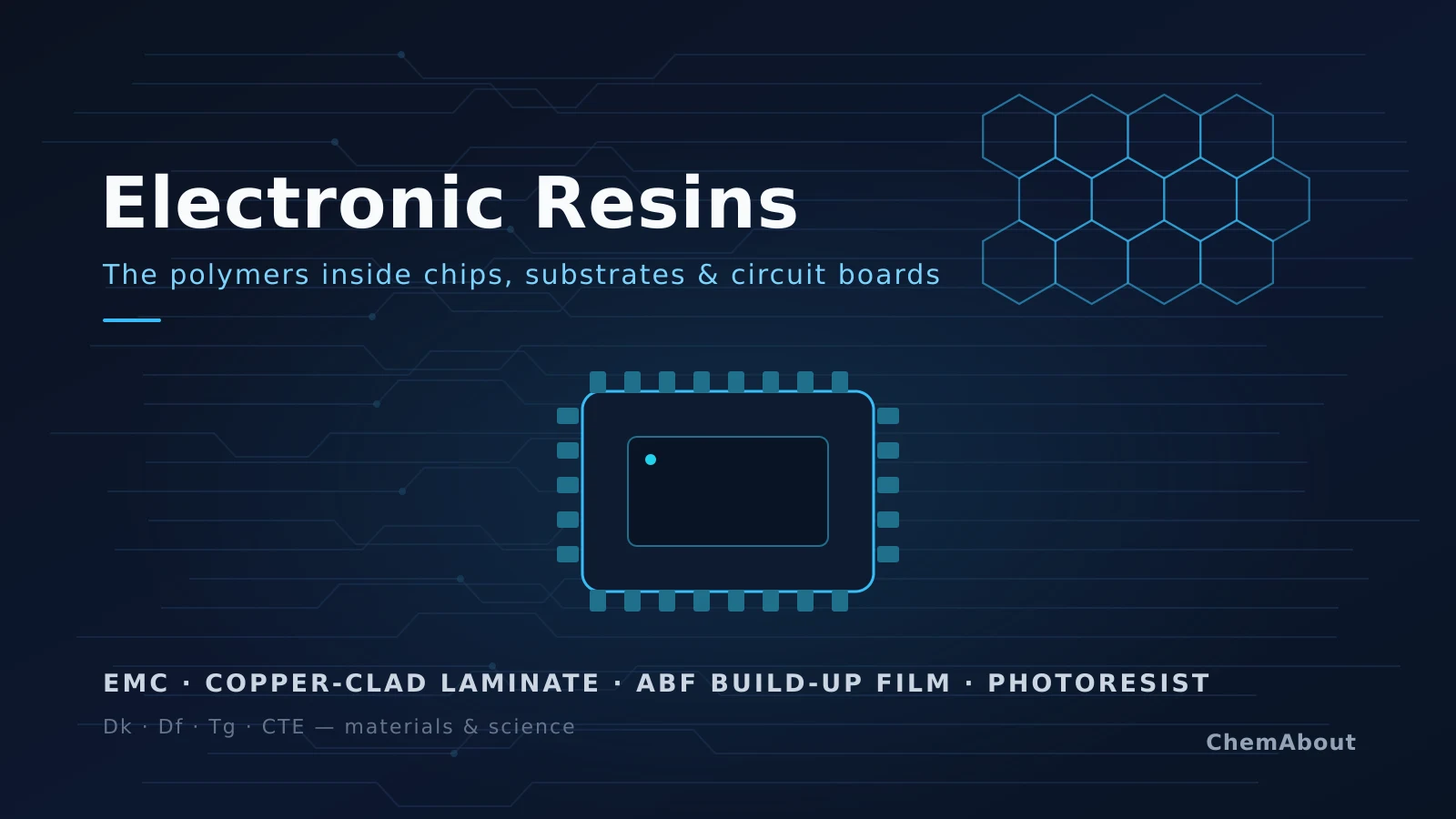
What Are Electronic Resins? The Polymers Inside Chips, Substrates, and Circuit Boards
8 min read
What Are Electronic Resins? The Polymers Inside Chips, Substrates, and Circuit Boards
"Electronic resin" is not a single substance. It is a working label for the family of electronic-grade polymer materials that insulate, support, encapsulate, and pattern the conductive parts of electronic devices. The same base chemistry — most often an epoxy — appears in very different forms: a powder pellet that is melted around a chip, a glass-cloth-reinforced sheet that becomes a circuit board, a thin film laminated to build up a package substrate, or a light-sensitive coating that defines circuit features.
What ties them together is not a fixed formula but a set of property targets. An electronic resin is judged by how it behaves electrically (how little it stores and dissipates a signal), thermally (how hot it can get before softening, and how well it conducts or expands with heat), and dimensionally (how much it moves relative to the silicon and copper around it). The chemistry is chosen to hit those numbers.
The base chemistry: thermosetting epoxies
Most electronic resins are thermosets. A thermoset starts as a liquid or fusible solid and is cured into a rigid, cross-linked network that will not melt again on reheating. The dominant chemistry is the epoxy resin, very often based on the diglycidyl ether of bisphenol A (DGEBA), a bifunctional epoxide.
Curing converts that small molecule into a dense polymer network. A multifunctional curing agent (hardener) — commonly polyamines, amidoamines, or phenolic compounds — opens the strained epoxide ring. With amine hardeners, the nitrogen performs a nucleophilic attack on the epoxide, forming a new carbon–nitrogen bond and a hydroxyl group (a β-hydroxy ether linkage); phenolic hardeners react analogously. Repeated across many sites, this produces a heavily cross-linked thermoset valued for mechanical strength, adhesion, and chemical resistance.
Because the network is fixed once cured, a thermoset such as a cured epoxy can pass through high-temperature steps — for example, a solder reflow profile reaching up to about 260 °C — without melting and flowing again. That heat resistance is one reason epoxy systems became the backbone of electronic packaging.
Encapsulation: epoxy molding compounds (EMC)
When a finished semiconductor die is sealed inside its black plastic body, the material doing the sealing is usually an epoxy molding compound. EMC is a formulation of a solid thermosetting epoxy resin, a phenolic-type curing agent, a large fraction of fine inorganic filler (typically fused silica, SiO₂), and additives such as flame retardants, coupling agents, mold-release agents, and stress modifiers.
In practice EMC is supplied as compressed solid pellets. In low-pressure transfer molding, the pellets are heated to a flowable state and forced through gates around the die and its wire bonds or bumps, then cured in place. The micron-scale silica gives the melt enough flow to fill narrow gaps while filling most of the final volume, which reduces thermal expansion and shrinkage. By industry accounts, more than 80% of semiconductor devices are encapsulated with epoxy molding compounds.
Property targets for EMC include low moisture uptake, low ionic contamination, a thermal expansion close to silicon, and increasingly high thermal conductivity and low warpage — the last two matter for power modules and large packages that must move heat and stay flat through assembly.
The circuit board: copper clad laminate resins
A rigid printed circuit board begins as copper clad laminate (CCL): copper foil bonded to an insulating dielectric, where the dielectric is a resin reinforced by a substrate such as woven glass cloth. The resin choice sets most of the board's electrical and thermal behavior. Reported dielectric resin classes include phenolic, epoxy, polyimide, polytetrafluoroethylene (PTFE), and bismaleimide-triazine (BT).
- Epoxy systems are the most common. The familiar "FR-4" grade is a glass-reinforced epoxy; flame retardancy has traditionally been provided by brominated epoxy resins, with halogen-free alternatives also in use.
- BT resin (bismaleimide-triazine, often blended with epoxy) offers higher heat resistance and has been widely used in IC packaging substrates.
- Polyimide resins, reinforced with glass, are used where high temperature stability and mechanical toughness are needed.
- PTFE, polyphenylene ether (PPE/PPO), cyanate ester, and hydrocarbon resins are used where signal loss must be minimized at high frequency (see below).
The key electrical descriptors are the dielectric constant (Dk), which scales how much a material slows and stores an electromagnetic signal, and the dissipation factor (Df, or loss tangent), which scales how much signal energy is lost as heat. Lower Dk and Df generally mean faster, lower-loss interconnect.
High-frequency and high-speed resins
As data rates and carrier frequencies rise — the 5G and high-speed-digital regime — the loss in the dielectric becomes a limiting factor. Here the resin families diverge by polarizability. Conventional epoxy, modified epoxy, cyanate ester, and polyimide have useful thermal and mechanical properties but generally cannot reach ultra-low loss (Df below ~0.003) at high frequency. PTFE, PPE, and some hydrocarbon resins can, because of their low molecular polarizability.
PTFE has a low dielectric constant (Dk on the order of 2.1) and very low loss, which is why it is a reference material for RF, microwave, and millimeter-wave boards; its trade-off is more demanding processing. Polyphenylene ether (PPE/PPO) is often described as second only to PTFE in dielectric performance while being easier to process, which has driven a range of modified PPE formulations for "very low loss" and "ultra low loss" high-speed laminates. Across these materials the recurring targets are low Dk, low Df, a low coefficient of thermal expansion (CTE), and adequate thermal conductivity.
The package substrate: build-up dielectric films
Between the silicon die and the circuit board sits the package substrate, and in high-performance processors its insulating layers are often a build-up dielectric film. The best-known is Ajinomoto Build-up Film (ABF), a filled resin film. It is produced by coating the resin in thicknesses of roughly 10–100 µm onto a PET carrier film, protected by a polypropylene cover sheet, and is laminated layer by layer to build high-density interconnect substrates.
ABF was first used to package an IC in 1999 and has since been the dielectric of choice for the substrates of high-performance CPUs, GPUs, FPGAs, and ASICs, where its thermal stability, low dielectric loss, and insulation reliability through repeated thermal cycling are the relevant properties. The Ajinomoto Group has reported holding the large majority of this specific market.
The patterning material: photoresists
Photoresists are electronic resins of a different purpose: rather than staying in the device, they are temporary, light-sensitive coatings that transfer a circuit pattern, then are removed. Their behavior is defined by how their solubility changes on exposure to light.
Classic positive-tone resists pair a novolak (a phenolic resin) with a diazonaphthoquinone (DNQ) photoactive compound. The DNQ makes the novolak resist dissolution in aqueous base; ultraviolet exposure converts the DNQ so the exposed regions become soluble and develop away. For the smaller features of deep-UV and extreme-UV (EUV) lithography, chemically amplified resists (CARs) are used: exposure generates an acid that catalyzes many deprotection reactions per absorbed photon, dramatically increasing sensitivity and enabling sub-10 nm features. The base polymers and protecting-group chemistry are tuned to each exposure wavelength.
The numbers that define an electronic resin
Across all of these forms, a consistent set of parameters describes whether a resin fits an electronic application:
- Dielectric constant (Dk) and dissipation factor (Df) — signal speed/storage and signal loss; lower is generally preferred for high-speed and high-frequency use.
- Glass transition temperature (Tg) — the temperature at which the cured resin softens from a glassy to a rubbery state, bounding the thermal range over which dimensions and stiffness are stable.
- Coefficient of thermal expansion (CTE) — how much the resin grows with temperature; mismatch against silicon and copper drives mechanical stress and warpage.
- Thermal conductivity — how well the material moves heat away from the die, increasingly important for power and high-performance devices.
- Flame retardancy — for example the UL-94 framework and grades such as FR-4, achieved with brominated or halogen-free chemistries.
- Moisture uptake and ionic purity — absorbed water and mobile ions affect insulation, reliability, and corrosion, so electronic grades are formulated for low values.
These targets explain why one word covers so many materials. An epoxy molding compound, an FR-4 laminate, an ABF layer, and a EUV photoresist share little in final shape or role, but each is an organic-polymer system engineered to a defined electrical, thermal, and dimensional specification — which is what "electronic resin" actually names.
References
- Sumitomo Bakelite: Epoxy Resin Molding Compounds for Encapsulation of Semiconductor Devices (SUMICON EME)
- Wikipedia: Epoxy molding compounds
- Shin-Etsu Chemical: Epoxy Encapsulant Material
- Wikipedia: Bisphenol A diglycidyl ether (DGEBA)
- PMC: Surface Chemistry and Molecular Dynamics of Epoxy Resin During Curing
- JLCPCB: What is Copper Clad Laminate (CCL)?
- PCBCart: A Comprehensive Introduction of Copper Clad Laminate
- MDPI/PMC: MPPE/SEBS Composites with Low Dielectric Loss for High-Frequency Copper Clad Laminates
- Cadence: Why Ajinomoto Build-Up Film (ABF) is Used in IC Packaging
- Polymer Innovation Blog: Build-Up Films for Flip Chip Semiconductor Substrates
- Shin-Etsu MicroSi: I-line / G-line / NOVOLAK and Chemically Amplified Resists
- RSC Polymer Chemistry: Emerging trends in polymeric resists for EUV lithography
Blog
Sourcing or supplying what you just read about?
ChemAbout connects chemical buyers and suppliers worldwide. Tell us what you need, or list what you offer.
Related articles

Article5 min read
Therapeutic Peptides in 2026: This Year's Breakthroughs
2026 has been a concentrated year for peptide therapeutics. Efficacy reached a new high in late-stage trials, the obesity field moved beyond the incretins to amylin, the oral route reached weight management, and peptide-guided radioligand therapy kept advancing — each point tied to a specific 2025–2026 result.
ArticleChemAbout Editorial Team4 min read
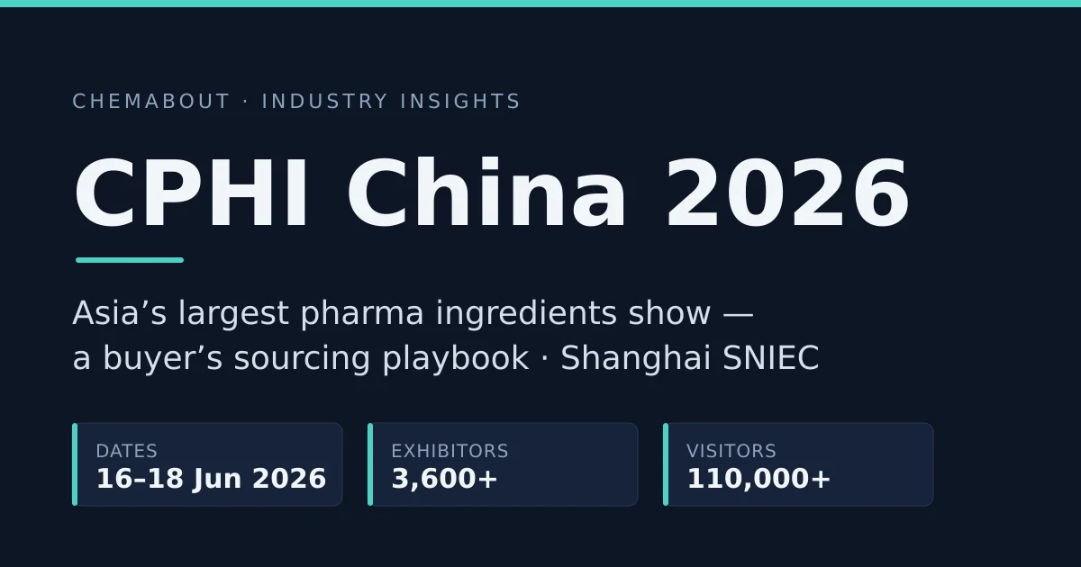
Asia's Biggest Pharma Show Is Back: A Sourcing Playbook for CPHI & PMEC China 2026
CPHI & PMEC China — 3,600+ exhibitors, 110,000+ visitors — opens 16 June at Shanghai's SNIEC. A practical playbook for buyers: go in with a shortlist, qualify suppliers on the floor, and fix the follow-up before you fly home.

ArticleChemAbout Editorial Team4 min read
REACH in 2026: Two New SVHCs and a PFAS Foam Deadline Worth Planning For
ECHA added n-Hexane and BPAF to the REACH Candidate List in February 2026, and the EU's PFAS firefighting-foam restriction hits its first hard deadline in October. Here's what to screen, what to ask suppliers, and which dates to put on your sourcing calendar.